
What’s electron microscopy?
Earlier than answering this query, we have to take a step again in historical past and acknowledge the work of the Dutch scientist Antoni van Leeuwenhoek (1632-1723) and Englishman Robert Hooke (1635-1703). Each performed instrumental roles within the identification of microorganisms utilizing glass lenses and primarily launched the fields of optical microscopy and microbiology. But with advances within the subject, German physicist Ernst Abbe acknowledged that optical microscopy can be restricted by a basic legislation of optical physics – the diffraction of sunshine – that will restrict the decision of optical microscopes. This was known as the “Abbe diffraction restrict”.1 Abbe deduced {that a} microscope couldn’t resolve two objects positioned nearer than λ/2NA, the place λ is the wavelength of sunshine and NA is the numerical aperture of the imaging lens. Central to this equation defining the decision restrict is the wavelength, λ. It’s immediately proportional to the achievable decision – the shorter the wavelength, the higher the decision. That is the hyperlink to electron microscopy.
Without the work of German physicist Hans Busch (1884-1973), improvement of electron microscopy would have been not possible. He was the primary to indicate {that a} magnetic subject might focus a beam of electrons in a way just like how glass lenses can focus seen gentle. Fellow German physicist Ernst Ruska (1906-1988) took notice of the work of Busch and utilized it to the event of the electron microscope, for which he received the 1986 Nobel Prize in Physics.2 He was additionally nicely conscious of the impression his discovery might have if the wavelength of the electrons might be lowered. French physicist Louis de Broglie (1892-1987) had already taken care of this utilizing the speculation of wave particle duality exhibiting that beams of electrons acted as waves with a wavelength that might be predicted based mostly on the rate of the electron. This might be adjusted by accelerating the electrons by means of {an electrical} potential (in apply this is called the accelerating voltage of the electron microscope). Electron wavelengths at completely different accelerating voltages are given in Desk 1.
Desk 1: Electron wavelengths at completely different electron accelerating voltages (the upper the voltage, the upper the rate of the electron).
|
Accelerating voltage (kV) |
Wavelength (pm) |
|
1 |
38.8 |
|
10 |
12.2 |
|
20 |
8.6 |
|
30 |
7.0 |
|
40 |
6.0 |
|
60 |
4.9 |
|
80 |
4.2 |
|
100 |
3.7 |
|
120 |
3.4 |
|
200 |
2.5 |
The impression on microscopy decision is now clear. The wavelength of the electrons listed within the desk is about 5 orders of magnitude decrease than that of the bottom wavelength of seen gentle (380,000 pm). Primarily based on the Abbe diffraction restrict equation given above, it will have an unlimited impact on the spatial decision. This was the theoretical driving pressure for the event of electron microscopy.
So, in any case that, we will reply our authentic query. Electron microscopy makes use of a beam of electrons centered by electromagnetic lenses to picture supplies of all sorts at spatial resolutions that far exceed these obtainable by commonplace optical microscopy. There are two frequent forms of electron microscopes: transmission electron microscopes (which was the kind developed by Ruska) and scanning electron microscopes. These two varieties have additionally been hybridized to provide scanning transmission electron microscopes and scanning electron microscopes outfitted with transmission detectors. But regardless of the maturation of the applied sciences, new technological developments proceed to push the bounds of decision ahead.3
Decision of electron microscopy
The decision of electron microscopy relies upon upon a number of components, central to which is the accelerating voltage as famous above. However different components are necessary as nicely, such because the magnetic lenses within the microscopes and the impact of aberrations in electromagnetic lenses.4 Decision limits for various varieties and class of electron microscopes are listed in Desk 2. Be aware that these fashionable TEM designs are capable of obtain atomic decision.
Desk 2: Spatial resolutions of varied forms of electron microscopes.
|
Sort of electron microscope |
Typical spatial decision |
|
Tabletop SEM (compact model can sit on a desk – thermal emission supply) |
~3 -15 nm |
|
Thermal emission electron supply SEM |
3 nm |
|
Schottky subject emission SEM |
0.6 nm |
|
120 kV TEM |
0.2 nm |
|
200 kV TEM |
0.1 nm |
|
300 kV TEM |
0.1 nm |
|
300 kV TEM with aberration correction |
0.06 nm |
Varieties of electron microscope and the way they work
Transmission electron microscopy (TEM)
In TEM, a beam of accelerated electrons is transmitted by means of the pattern, interacting with the pattern in varied methods to acquire various kinds of data, earlier than being detected by a phosphor display, movie or semiconductor-based detectors under the pattern. Because the beam is transmitted by means of the pattern, there are two fundamental necessities in TEM. First, the accelerating voltage have to be sufficiently excessive that the beam of electrons can cross by means of the pattern with out being absolutely absorbed, and secondly, to help with this requirement, the samples have to be skinny, usually 100 nm in thickness. This latter requirement is a perform of the common atomic variety of the pattern. Heavier components that make up metals and alloys will probably be stronger electron absorbers and fewer lenient when it comes to pattern thickness. However, organic samples, which consist primarily of C, H, O, N and these low atomic quantity components, don’t readily take in the electrons and may thus accommodate thicker samples. Organic samples are often ready by ultramicrotomy, the place samples are embedded right into a plastic resin after which sectioned utilizing a microtome with both a glass or diamond knife. Inorganic supplies may additionally be ready this manner, however extra typically they’re reduce into 3 mm disks, mechanically polished after which lastly thinned to perforation with an ion beam or with an electrolytic answer. It’s the areas across the perforation that will probably be skinny sufficient for electron transmission. A slight drawback is that these samples will probably be step by step thicker as you progress farther from the purpose of perforation, so pattern thickness results will cut back transmission. Alternatively, one can use a centered ion beam instrument to select a selected space of the pattern, take away it, connect to a TEM pattern provider and skinny it right down to ~100 nm utilizing a centered Ga+ ion beam. This has the benefit of precision pattern web site choice and producing comparatively uniform thickness samples. Nevertheless, the instrumentation is dear and a substantial amount of operator talent is required.
A schematic diagram depicting the most important electron optical components of a TEM is proven in Determine 1. In (a), operation of the TEM in brilliant subject imaging mode is proven. This begins on the high of the instrument with a supply of electrons, mostly both a W-filament (the place electrons are thermally emitted) or a subject emission supply (the place excessive potentials are utilized to extract the electrons from the supply tip). Subject emission sources could also be thermally assisted (known as Schottky subject emission sources) or not (known as chilly subject emission sources). A set of condenser lenses are then used to form the beam onto and thru the pattern. Focusing of the picture takes place after the beam has handed by means of the specimen utilizing a set of lenses (goal, intermediate and projector lenses). The ultimate picture is shaped on a fluorescent display (the impression of electrons inflicting the emission of sunshine), photographic movie or semiconductor-based detectors (e.g., charge-couple units (CCDs)).

Determine 1: Schematic diagram of a TEM in (a) brilliant subject imaging mode and (b) electron diffraction mode.
Nevertheless, photographs are usually not of a lot use until they present some type of distinction. There are other ways by which distinction is shaped in a TEM. For instance, many forms of samples imaged in a TEM will probably be crystalline in nature, and topic of the legal guidelines of electron diffraction given by the Bragg equation:
nλ = 2dsinθ
The place λ is the wavelength of the electrons, d is the spacing between lattice planes of a selected orientation, θ is the Bragg diffraction angle and n is the order of reflection. Utilizing a TEM at 200 kV accelerating voltage, the wavelength is (Desk 1) 0.00251 nm. Utilizing the crystallographic planes of atoms within the steel Cu with the biggest spacing between planes (the (111) plane of Cu) for example, with a d-spacing of 0.207 nm, we will resolve for sinθ.
Sinθ = .00251 nm / 2 x 0.207 nm = 0.0061; θ = .35°
What this tells us is that the Bragg angle for diffraction is sort of parallel to the electron beam. Which means that crystallographic planes will diffract depth away from the in any other case transmitted beam when they’re aligned practically parallel to the electron beam. This manifests itself as a darker space on the picture display or movie. One of these distinction is known as diffraction distinction, and one can be taught a fantastic deal in regards to the crystallographic make-up of the samples utilizing this type of distinction. Moreover, as samples may be tilted within the TEM, one can produce a collection of photographs the place completely different crystallographic planes are introduced into the Bragg situation for diffraction to offer much more data.
The electron diffraction sample can in actual fact be recorded by the TEM by working it in a barely completely different method. The target aperture that’s inserted slightly below the target lens in Determine 1a is eliminated to permit the diffracted beams to be transmitted. The lenses under are configured in a barely completely different method to permit the diffracted beams to be projected onto the picture display together with the extreme transmitted beam centered within the diffraction sample. The gap between the pattern and the display is understood, as is the wavelength. These patterns may be listed to realize crystallographic data and in addition assist with compound identification, as all compounds could have particular crystal buildings and lattice spacings that may be decided from the patterns and matched to information in available crystallographic libraries5 for which most tutorial establishments could have a license or no less than the old fashioned card catalogues.
A second kind of distinction formation that generally happens is that of atomic quantity distinction. In its easiest kind, this refers back to the case the place the electrons are absorbed by some excessive atomic quantity aspect within the pattern, changing their power to warmth. As soon as absorbed, these electrons can’t transmit by means of the pattern, and we’re left with a darker space on the picture display under. Nevertheless, as a result of electrons accelerated with excessive voltages and skinny samples are used, this type of atomic quantity distinction just isn’t probably the most prevalent. Extra more likely to happen is an interplay of the negatively charged electron beam with the constructive potential of the nucleus which is able to scatter the trajectory of the electron and once more result in an depth deficit on the imaging display.
Neither of those mechanisms are more likely to happen in a organic pattern, as they usually don’t present excessive levels of crystallinity, and nor do they usually present a substantial amount of atomic quantity distinction, being primarily composed of low atomic quantity components resembling C, N, O and H. To help distinction, decrease accelerating voltages are sometimes used, however extra importantly the samples bear an extra step throughout preparation known as staining. Although there are lots of completely different recipes for staining organic samples, a generally used mixture is uranyl acetate and lead citrate. Be aware each include the heavy metals, U and Pb which would be the distinction formers. These two stains will bind to completely different buildings within the cell and their use offers the distinction required to establish the completely different organelles inside cells and tissues. The result’s a TEM picture resembling that proven in Determine 2 of a human mast cell.

Determine 2: Instance of a organic pattern, excessive stress frozen, stained with uranyl acetate and lead citrate and visualized by TEM. Wild kind Human mast cell line 1 (HMC-1); Picture exhibits the nucleus of the cells and the black arrow signifies nuclear envelope budding occasions. Credit score: Johanna Höög, Dimitra Panagaki and Jacob Croft, reproduced underneath the Creative Commons Attribution 3.0 Unported (CC BY 3.0) license.
The important thing data that may be gained from TEM and pattern necessities are summarized under:
● Pictures with very excessive spatial decision (~ 0.04 nm on excessive finish fashionable devices, simply reaching atomic decision).
● Crystallographic data together with direct imaging of crystal lattice defects and faults in crystalline supplies.
● Electrons must be accelerated at excessive voltages (often 100-200 kV however can vary from 40-300 kV on industrial devices).
● Samples must be skinny to permit for electron transmission by means of the samples (~100 nm).
● Organic samples want some type of heavy steel staining, with protocols utilizing uranyl acetate and lead citrate being the most typical.
Scanning electron microscopy (SEM)
The scanning electron microscope is the kind of electron microscope with which most of us are in all probability extra acquainted. These photographs we see of the compound eye of a fly had been acquired utilizing an SEM. However apparently, their improvement lagged a bit of in comparison with TEM. An exquisite historical past of the early improvement of SEM is supplied by McMullan.6
There are two chief variations between an SEM and a TEM. In an SEM, the centered electron beam is scanned within the x-y instructions throughout the pattern. The beam within the TEM just isn’t scanned until utilized in scanning transmission electron microscopy (STEM – see subsequent part). Secondly, there is no such thing as a requirement that the pattern be skinny. The floor of the pattern is what’s examined and maybe the one limitation of the pattern is that it should be capable to be inserted or match throughout the evaluation chamber.
A schematic diagram of an SEM is proven in Determine 3 and consists of most of the identical components because the TEM. It begins with a supply of electrons on the high of the column which, once more, could also be a W filament thermal emission supply or a Schottky thermally assisted subject emission supply. Some devices do use a chilly subject emission supply, however these are the exception greater than the norm. And identical to the TEM there’s a collection of condenser lenses that help in shaping the beam and adjusting the beam present that may ultimately impinge on the pattern. A strip of apertures additionally assists on this – smaller apertures will result in smaller beam currents and beam diameters (which in the end determines the spatial decision). The scan coils raster the beam throughout the pattern in dimensions chosen by the consumer by means of choice of the magnification, whereas the chosen sign is detected in synchronicity with the raster. The next magnification scans the beam throughout more and more smaller areas. The target lens focuses the beam to the best diameter doable. The smaller the beam diameter, the finer the options of the pattern that may be resolved. With fashionable devices, the world of the column across the goal lens has been modified and we are going to return to this within the “Detectors in SEM” part.

Determine 3: Schematic diagram of an SEM.
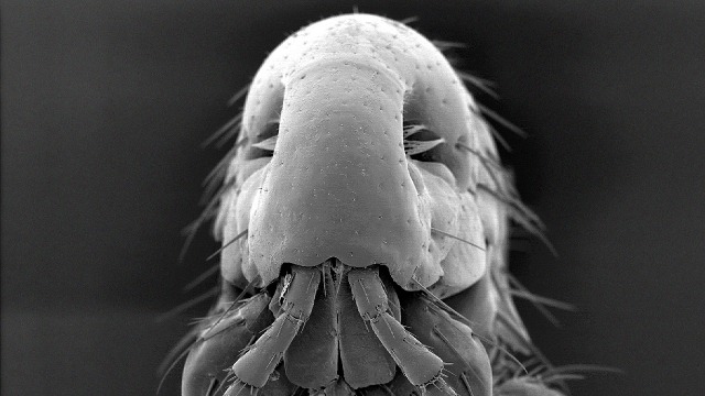
An instance of the 3D nature of photographs supplied by SEM is illustrated by the stereoocilia bundle of the inside ear proven in Determine 4.

Determine 4: Instance of an SEM picture. An SEM picture of the sensory hair bundle of a single hair cell from a terrapin’s listening to organ within the inside ear. Vibrations made by sound trigger the hairs to be moved forwards and backwards, alternately stimulating and inhibiting the cell. When the cell is stimulated it causes nerve impulses to kind within the auditory nerve, sending messages to the mind. Credit: Dr. David Furness reproduced underneath the Creative Commons Attribution 3.0 Unported (CC BY 3.0) license.
SEM amenities are present in tutorial, industrial and industrial facilities worldwide. There are in all probability no supplies that haven’t been examined in an SEM earlier than. Purposes embrace those who one would anticipate – biology, supplies science and nanotechnology – but additionally in fields resembling forensics,7 artwork conservation8 and cosmetics.9
The electron beam/pattern interplay quantity
When an lively electron beam strikes a pattern, many various alerts originating from completely different depths from the pattern floor are produced. These may be detected and exploited to offer a wealth of details about the pattern. This beam-sample interplay, and the primary alerts it produces, are proven in Determine 5.
- Auger electrons are low power electrons emitted from the close to floor area of the pattern and have energies attribute of the weather from which they’re emitted. They’re used solely in Auger electron spectroscopy devices somewhat than SEM’s.
- Secondary electrons originate from deeper throughout the pattern and are a results of inelastic scattering of the first beam. The first beam interacts with electrons within the pattern and imparts a few of its power to them. These secondary electrons might exit the pattern and be detected. These electrons are additionally of usually low power and supply a wealth of details about the topography of the samples.
- Lastly, there’s the case the place once more the first electron interacts with the nucleus of atoms within the pattern and its trajectory is reversed again away from the specimen. These are known as backscattered electrons, emanate from better depths throughout the pattern and are of a lot larger power, being successfully elastically scattered. Because of this, backscattered electron photographs can provide qualitative details about the relative atomic variety of the weather current within the pattern.
- Nonetheless deeper into the beam/pattern interplay quantity, attribute X-rays are additionally generated which can be used to quantitatively decide the chemical composition of the pattern.

Determine 5: Electron beam/pattern interplay produces varied alerts from completely different depths throughout the pattern. Auger electrons, secondary electrons, backscattered electrons and attribute X-rays.
The depths of emission of those completely different alerts just isn’t fixed and relies upon very extremely on the accelerating voltage of the electron beam and the pattern composition. The everyday pear- formed quantity from which these alerts originate will probably be confined nearer to the pattern floor the decrease the accelerating voltage and the upper the atomic quantity. That is significantly essential for attribute X-ray emission. When the electron beam strikes the pattern, it could actually knock electrons out of inside shell orbitals. These vacancies are then stuffed by electrons from the outer shells and within the course of, emit X-rays which are attribute of the aspect from which it originated. That is the idea of an ancillary microbeam evaluation approach that is quite common on SEM’s – power dispersive X-ray evaluation (EDS or EDX). Nevertheless, the quantity the place X-ray era happens is far bigger than the diameter of the electron beam, so if we had been to detect and map the distribution of the attribute X-rays of the weather within the pattern, the spatial decision will rely upon the scale of that interplay quantity and never the diameter of the electron beam. A method to enhance that is to decrease the accelerating voltage. This reduces the scale of that interplay quantity and improves the spatial decision of the X-ray maps.
Detectors in SEM
Each SEM could have an Everhart-Thornley secondary electron detector, which makes use of a positively biased Faraday cage to draw secondary electrons. These electrons are accelerated in the direction of a scintillator the place they produce photons, that are funneled right into a photomultiplier tube the place the sign is amplified and measured. By making use of a small constructive voltage to the Faraday cage, one can filter out the low power electrons and detect solely the upper power backscattered electrons. Nevertheless, this apply just isn’t as frequent because it as soon as was because of the improvement of solid-state backscattered detectors, that are usually ring-type detectors fitted immediately underneath the target lens or positioned on a piston that may be inserted and retracted to that very same location (see Determine 6 – retractable backscattered electron detector). Be aware that these backscattered electrons are additionally topic to Bragg’s legislation of diffraction and with cautious pattern preparation, crystallographic data will also be obtained. That is the idea for the approach often known as electron backscattered diffraction, or EBSD.
Most fashionable SEM’s could have a number of “in-lens” detectors. One of these configuration is proven in Determine 6. On this case, the magnetic subject ensuing from the electromagnetic goal lens and the electrostatic lens is utilized to gather and funnel the low power secondary electrons again up the column for detection. The magnetic subject is very environment friendly at amassing these low power electrons and so this detector, very similar to the backscatter in-lens detector, could be very helpful when working at very low accelerating voltages (100 V to 3-5 kV) the place the pattern have to be inside a couple of mm of the target lens to take care of a finely centered electron beam. Nevertheless, this may occasionally even be one of many disadvantages of the in-lens detectors, as it’s precisely these very low power electrons that will probably be most prone to pattern charging artefacts, which happen when the pattern just isn’t grounded and builds up cost throughout evaluation. That is frequent when insulating samples are analyzed and resolved by the applying of a skinny (5-10 nm) movie of carbon or some conducting steel (Au, Pd and Pt are generally used) utilizing an evaporation or sputter coater that may be a frequent accent in each SEM laboratory.

Determine 6: Schematic diagram of the area across the goal lens of a contemporary SEM, exhibiting twin electromagnetic and electrostatic lenses and the trajectory of the secondary electrons collected by the actions of those two lenses again up the column to the higher secondary electron and backscattered electron detectors.
The important thing data that we will acquire from an SEM and any particular pattern necessities are summarized under:
● Excessive spatial decision of pattern surfaces (~ 0.5 nm) offering third-dimensional topographic data with secondary electrons.
● Qualitative compositional variations in samples utilizing backscattered electrons (one may additionally receive crystallographic data with EBSD detectors).
● May be very floor delicate when used at low voltages owing to the discount of the electron beam/pattern interplay quantity.
● In-lens detectors are very efficient underneath these situations.
● Quantitative elemental evaluation doable utilizing EDS.
● There’s actually no restrict to the pattern measurement, apart from it should be capable to be launched into and match within the evaluation chamber.
Scanning transmission electron microscopy (STEM)
STEM is just about precisely what it appears like – a mixture of TEM and SEM. In reality, most TEM’s as we speak are mixture programs that may be operated in both TEM or STEM mode. Like TEM, the samples nonetheless must be electron clear, however the addition of the power to raster the beam in a TEM permits using further alerts that can’t be spatially coordinated in standard TEM. These embrace scattered major beam electrons, attribute X-rays and electron power loss occasions. The distinctive spatial decision of the TEM is maintained, with the electron beam centered to a small diameter on the pattern floor. Attribute X-rays may be detected and mapped simply as they’re in an SEM. Nevertheless, the difficulty of the scale of the interplay quantity disappears as a result of the pattern is skinny. When electrons produce an X-ray, they lose the equal quantity of power and when an electron power loss spectrometer (EELS) is connected to the instrument, the loss occasions will also be mapped as a perform of place on the pattern. EELS has two principal strengths over EDS – the maps could have a barely higher spatial decision and it’s a approach delicate to the chemical setting and may subsequently present details about bonding and oxidation states just like X-ray photoelectron spectroscopy (XPS), however at considerably larger spatial decision.
Purposes of STEM attain many numerous fields of analysis, together with biology,10 and nanotechnology.11
Reflection electron microscopy (REM)
Reflection electron microscopy is a type of electron microscopy that additionally has its origins from Ernst Ruska.12 REM is mostly carried out in a TEM however by tilting the pattern such that the electron beam is at close to grazing incidence to the pattern floor. The pattern subsequently now not must be skinny and electron clear. Because of this, the interplay of the beam with the pattern is way much less and the resultant data obtained is from the very pattern floor. It’s subsequently a way used to review crystal surfaces. Examples of purposes embrace the examine of floor topography, statement of floor buildings, floor adsorption and oxidation processes.13 It’s considerably of a specialised technique that isn’t practically as generally used as SEM, TEM and STEM.
Freeze fracture electron microscopy
Freeze-fracture electron microscopy is a TEM-based technique utilized in organic research and is especially precious as a way of imaging membrane construction. When organic samples are within the frozen state, membranes have a airplane of weak point of their hydrophobic inside. If the pattern is then fractured, it’s going to achieve this alongside that airplane of weak point and sometimes break up the membrane into two halves, every similar to a phospholipid monolayer with related proteins. This produces a three-dimensional perspective of the membranous group of the cell, together with views of the membrane inside. These particulars are made seen within the electron microscope by evaporating Pt on to the specimen at an angle, successfully making a Pt-C reproduction of the fracture airplane.
There are 4 principal steps in making an ordinary freeze-fracture reproduction:
i) Fast freezing of the specimen
ii) Fracturing the specimen at low temperature (-100 °C or decrease)
iii) Make the reproduction of the newly uncovered frozen floor by vacuum-deposition of Pt and C
iv) Clear the reproduction utilizing bleach or acids to take away the organic materials
A full process is given by Severs.14 A typical picture exhibiting the distributions of lipid droplets surrounding the endoplasmic reticulum in a macrophage is proven in Determine 7.

Determine 7: Instance of freeze fracture electron microscopy picture exhibiting lipid droplets (LD) and endoplasmic reticulum in a macrophage. Credit score: From Robenek and Severs,15 reproduced underneath the Creative Commons Attribution 2.0 Generic (CC BY 2.0) license.
Current developments within the subject: Cryo EM
Cryo EM is a workflow/microscopy that has been developed to handle a longstanding concern in organic electron microscopy — how to have a look at organic samples of their native state. The impression of the event of Cryo EM was acknowledged in 2017 by being awarded the Nobel Prize in Chemistry.16 This has at all times been a difficulty as organic samples include a big fraction of water, which is eliminated throughout typical pattern preparation protocols resembling chemical fixation or freeze drying. In Cryo EM, the pattern is maintained at cryogenic temperatures all through all phases of pattern preparation and TEM evaluation. The strategy is particularly helpful for learning protein construction within the native state, and maybe most famously, no less than not too long ago, figuring out the buildings of the proteins within the spikes17 of the novel coronavirus.18 An instance of how Cryo EM can be utilized to amass photographs of samples resembling micro organism, and in addition its use in Cryo EM tomography to provide 3D reconstruction photographs is proven in Determine 8.19 That is achieved by merely buying quite a few photographs of the identical part at completely different angles of incidence to the electron beam.

Determine 8: Use of cryo EM tomography to picture the inside construction of bacterial cells. (a,b) Illustration of spiral structure of the nucleoid in micro organism exhibiting (a) a 21 nm thick tomographic slice by means of the 3D quantity of a cell and (b) a 3D floor rendering of the identical cell, with the spiral nucleoid highlighted (yellow). (c) Greater magnification view of a tomographic slice by means of the cell, exhibiting well-separated nucleoid spirals and ribosomes (darkish dots) distributed on the fringe of the nucleoid. (d) Expanded views of 21 nm thick tomographic slices, exhibiting top-views of polar chemoreceptor arrays. A schematic mannequin (inset) illustrates the spatial association of the chemoreceptor arrays within the airplane of the membrane. Credit score: Milne et al. 19
Current developments within the subject: In-situ TEM
One other space of analysis that’s garnering a lot consideration not too long ago is that of in-situ TEM, the place dynamic processes are being adopted at close to atomic scale20 by means of the event of specialised environmental holders for TEM. Biomineralization processes may be adopted in-situ which can present perception in bone therapeutic and restore of arduous tissue.21 The function of micro organism within the biking of metals within the setting22 has additionally been adopted utilizing in-situ TEM, the outcomes of which can have necessary implications in environmental science. Host-pathogen interactions23 have additionally been studied which supplied new data on the principles of engagement. An oxidation phenomenon of the Ni-based alloy 600, utilized in pressurized water reactor nuclear energy24 programs, has additionally been studied and new processes that will have an effect on the stress corrosion cracking conduct had been noticed.
References
1. Past the diffraction restrict. Nat Photonics. 2009;3(7):361-361. doi:10.1038/nphoton.2009.100
2. The Nobel Prize. https://www.nobelprize.org/prizes/physics/1986/summary/. Accessed August 25, 2021.
3. Courtland R. The microscope revolution that’s sweeping by means of supplies science. Nature. 2018;563(7732):462-464. doi:10.1038/d41586-018-07448-0
4. Rose HH. Historic facets of aberration correction. J Electron Microsc (Tokyo). 2009;58(3):77-85. doi:10.1093/jmicro/dfp012
5. Worldwide Centre for Diffraction Information. https://www.icdd.com/. Accessed August 25, 2021.
6. McMullan D. Scanning electron microscopy 1928–1965. Scanning. 1995;17(3):175-185. doi:10.1002/sca.4950170309
7. Basu S. Scanning Electron Microscopy in Forensic Science. In: Encyclopedia of Analytical Chemistry. John Wiley & Sons, Ltd; 2006. doi:10.1002/9780470027318.a1122
8. Zagora J. SEM-EDX Pigment Evaluation and Multi-Analytical Examine of the Floor and Paint layers of Francesco Fedrigazzi’s portray from Kostanje. CeROArt. 2013;(EGG 3). doi:10.4000/ceroart.3248
9. Kaliyadan F, Gosai B, Al Melhim W, et al. Scanning electron microscopy examine of hair shaft injury secondary to beauty remedies of the hair. Int J Trichology. 2016;8(2):94. doi:10.4103/0974-7753.188035
10. Sousa AA, Leapman RD. Improvement and software of STEM for the organic sciences. Ultramicroscopy. 2012;123:38-49. doi:10.1016/j.ultramic.2012.04.005
11. van den Bos KHW, Altantzis T, De Backer A, Van Aert S, Bals S. Current breakthroughs in scanning transmission electron microscopy of small species. Adv Phys X. 2018;3(1):1480420. doi:10.1080/23746149.2018.1480420
12. Ruska E. Die elektronenmikroskopische Abbildung elektronenbestrahlter Oberflachen. Zeitschrift fur Phys. 1933;83(7-8):492-497. doi:10.1007/BF01338960
13. Yagi Ok. Reflection electron microscopy. J Appl Crystallogr. 1987;20(3):147-160. doi:10.1107/S0021889887086916
14. Severs NJ. Freeze-fracture electron microscopy. Nat Protoc. 2007;2(3):547-576. doi:10.1038/nprot.2007.55
15. Robenek H, Severs NJ. Current advances in freeze-fracture electron microscop: the reproduction immunolabeling approach. Biol Proced On-line. 2008;10(1):9-19. doi:10.1251/bpo138
16. The Nobel Prize. https://www.nobelprize.org/prizes/chemistry/2017/press-release/. Accessed August 25, 2021.
17. Wrapp D, Wang N, Corbett KS, et al. Cryo-EM construction of the 2019-nCoV spike within the prefusion conformation. Science (80- ). 2020;367(6483):1260-1263. doi:10.1126/science.abb2507
18. Partitions AC, Park Y-J, Tortorici MA, Wall A, McGuire AT, Veesler D. Construction, Perform, and Antigenicity of the SARS-CoV-2 Spike Glycoprotein. Cell. 2020;181(2):281-292.e6. doi:10.1016/j.cell.2020.02.058
19. Milne JLS, Borgnia MJ, Bartesaghi A, et al. Cryo-electron microscopy – a primer for the non-microscopist. FEBS J. 2013;280(1):28-45. doi:10.1111/febs.12078
20. Pu S, Gong C, Robertson AW. Liquid cell transmission electron microscopy and its purposes. R Soc Open Sci. 2020;7(1):191204. doi:10.1098/rsos.191204
21. He Ok, Sawczyk M, Liu C, et al. Revealing nanoscale mineralization pathways of hydroxyapatite utilizing in situ liquid cell transmission electron microscopy. Sci Adv. 2020;6(47):eaaz7524. doi:10.1126/sciadv.aaz7524
22. Couasnon T, Alloyeau D, Ménez B, Guyot F, Ghigo J-M, Gélabert A. In situ monitoring of exopolymer-dependent Mn mineralization on bacterial surfaces. Sci Adv. 2020;6(27):eaaz3125. doi:10.1126/sciadv.aaz3125
23. Dearnaley WJ, Schleupner B, Varano AC, et al. Liquid-cell electron tomography of organic programs. Nano Lett. 2019;19(10):6734-6741. doi:10.1021/acs.nanolett.9b01309
24. Burke MG, Bertali G, Prestat E, Scenini F, Haigh SJ. The appliance of in situ analytical transmission electron microscopy to the examine of preferential intergranular oxidation in Alloy 600. Ultramicroscopy. 2017;176:46-51. doi:10.1016/j.ultramic.2016.11.014


