
Business’s first complete 3D-IC platform for multi-chiplet design and superior packaging Highlights:
-
Integrity 3D-IC integrates design planning, implementation and system evaluation in a single, unified cockpit
-
Designers can obtain system-driven PPA by way of the supply of built-in thermal, energy and static timing evaluation capabilities
-
Cadence’s third-generation 3D-IC resolution helps a variety of software areas, together with hyperscale computing, shopper, 5G communications, cellular and automotive
SAN JOSE, Calif., October 07, 2021–(BUSINESS WIRE)–Cadence Design Methods, Inc. (Nasdaq: CDNS) at this time introduced the supply of the Cadence® Integrity™ 3D-IC platform, the trade’s first complete, high-capacity 3D-IC platform that integrates 3D design planning, implementation and system evaluation in a single, unified cockpit. The Integrity 3D-IC platform underpins Cadence’s third-generation 3D-IC resolution, offering clients with system-driven energy, efficiency and space (PPA) for particular person chiplets by way of built-in thermal, energy and static timing evaluation capabilities.
This press launch options multimedia. View the total launch right here: https://www.businesswire.com/news/home/20211006006020/en/

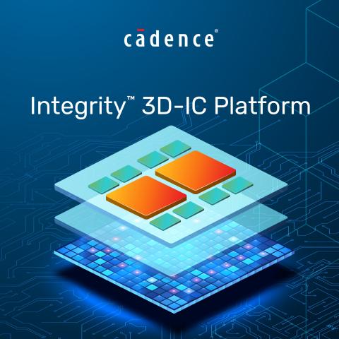
The Cadence® Integrity™ 3D-IC platform is the trade’s first complete, high-capacity 3D-IC platform that integrates 3D design planning, implementation and system evaluation in a single, unified cockpit. (Graphic: Enterprise Wire)
Chip designers creating hyperscale computing, shopper, 5G communications, cellular and automotive purposes can obtain higher productiveness with the Integrity 3D-IC platform versus a disjointed die-by-die implementation method. The platform uniquely gives system planning, built-in electrothermal, static timing evaluation (STA) and bodily verification flows, enabling quicker, high-quality 3D design closure. It additionally incorporates 3D exploration flows, which take 2D design netlists to create a number of 3D stacking situations primarily based on consumer enter, robotically choosing the optimum, ultimate 3D stacked configuration. Moreover, the platform database helps all 3D design varieties, letting engineers create designs at a number of course of nodes concurrently and carry out seamless co-design with bundle design groups and outsourced semiconductor meeting and check (OSAT) firms that use Cadence Allegro® packaging applied sciences. For extra info on the Integrity 3D-IC platform, please go to www.cadence.com/go/integrity.
Prospects utilizing the Integrity 3D-IC platform have entry to the next options and advantages:
-
Frequent cockpit and database: Lets SoC and bundle design groups co-optimize the entire system concurrently, permitting system-level suggestions to be included effectively.
-
Full planning system: Incorporates a whole 3D-IC stack planning system for every type of 3D designs, enabling clients to handle and implement native 3D stacking.
-
Seamless implementation instrument integration: Offers ease of use by way of direct script-based integration with the Cadence Innovus™ Implementation System for high-capacity digital designs with 3D die partitioning, optimization and timing flows.
-
Built-in system-level evaluation capabilities: Allows strong 3D-IC design by way of early electrothermal and cross-die STA, which permits early system-level suggestions for system-driven PPA.
-
Co-design with the Virtuoso® Design Atmosphere and Allegro packaging applied sciences: Permits engineers to seamlessly transfer design knowledge from Cadence analog and packaging environments to completely different elements of the system by way of the hierarchical database, enabling quicker design closure and improved productiveness.
-
Simple-to-use interface: Features a highly effective consumer cockpit with a move supervisor that gives designers with a uniform, interactive approach to run related system-level 3D system evaluation flows.
“Cadence has traditionally provided clients sturdy 3D-IC packaging options by way of its main digital, analog and bundle implementation product strains,” stated Dr. Chin-Chi Teng, senior vp and basic supervisor within the Digital & Signoff Group at Cadence. “With latest developments in superior packaging applied sciences, we noticed a must additional construct upon our profitable 3D-IC basis, offering a extra tightly built-in platform that ties our implementation expertise with system-level planning and evaluation. Because the trade continues to maneuver towards completely different configurations of 3D stacked dies, the brand new Integrity 3D-IC platform lets clients obtain system-driven PPA, lowered design complexity and quicker time to market.”
The Integrity 3D-IC platform is a part of the broader Cadence 3D-IC resolution portfolio, which matches past digital and contains system and verification and IP options. The broader resolution gives {hardware} and software program co-verification and energy evaluation of the total system by way of the Dynamic Duo, which consists of the Palladium® Z2 and Protium™ X2 platforms. It additionally gives connectivity by way of chiplet-based PHY IP with PPA optimized for latency, bandwidth and energy. The Integrity 3D-IC platform provides co-design capabilities with the Virtuoso Design Atmosphere and Allegro applied sciences, built-in IC signoff extraction and STA with the Quantus™ Extraction Resolution and Tempus™ Timing Signoff Resolution, and built-in sign integrity/energy integrity (SI/PI), electromagnetic interference (EMI) and thermal evaluation with the Sigrity™ expertise portfolio, Readability™ 3D Transient Solver and Celsius™ Thermal Solver. Each the brand new Integrity 3D-IC platform and the broader 3D-IC resolution portfolio are constructed on a strong basis of SoC design excellence and system-level innovation, supporting the corporate’s Clever System Design™ technique. For extra info on the Cadence 3D-IC resolution, go to www.cadence.com/go/3DIC.
Endorsements
“With 3D-IC design persevering with to achieve momentum, there’s an elevated must automate the planning and partitioning of a 3D stack die system extra effectively. Because the world-leading analysis and innovation hub in nanoelectronics and digital applied sciences and thru our longstanding collaboration with Cadence, we’ve efficiently discovered automated methods to partition designs to construct an optimum 3D stack with elevated accessible reminiscence bandwidth that pushes efficiency and lowers energy in advanced-node designs. The built-in reminiscence on the logic move included in Cadence’s Integrity 3D-IC platform permits cross-die planning, implementation and multi-die STA, which our analysis groups demonstrated on a multi-core high-performance design.”
-Eric Beyne, senior fellow and program director, 3D System Integration, imec
“To push AI acceleration utilizing optical computing, we’ve constantly leveraged all the newest, modern traits within the chip design trade—a key innovation being multi-chiplet stacking. As a way to construct a heterogenous multi-chiplet stacked design, it is very important have a completely built-in planning and implementation system, which might characterize a number of expertise nodes in a single cockpit. The Cadence Integrity 3D-IC platform gives a unified database resolution with implementation and early system-level evaluation capabilities, together with timing signoff and electrothermal evaluation. It helps us ship next-generation innovation utilizing optical computing for AI acceleration.”
– Ph.D Yichen Shen, founder and CEO of Lightelligence Inc.
“There are elevated necessities for constructing 2.5D/3D-IC designs with a number of chiplets like logic dies and high-bandwidth recollections which can be related with silicon interposer expertise. To satisfy our efficiency standards, interposer routing wants automation to be correct-by-construction whereas considering location, shielding and system integrity necessities. The Cadence Integrity 3D-IC platform is properly built-in for optimum interposer implementation and system evaluation and provides quick, full system evaluation, enabling us to ship designs that meet reminiscence bandwidth calls for for hyperscale computing and 5G communications.”
-Tuobei Solar, R&D head, Division of Packaging and Testing, SaneChips
About Cadence
Cadence is a pivotal chief in digital design, constructing upon greater than 30 years of computational software program experience. The corporate applies its underlying Clever System Design technique to ship software program, {hardware} and IP that flip design ideas into actuality. Cadence clients are the world’s most modern firms, delivering extraordinary digital merchandise from chips to boards to programs for probably the most dynamic market purposes, together with shopper, hyperscale computing, 5G communications, automotive, cellular, aerospace, industrial and healthcare. For seven years in a row, Fortune journal has named Cadence one of many 100 Finest Firms to Work For. Study extra at cadence.com.
© 2021 Cadence Design Methods, Inc. All rights reserved worldwide. Cadence, the Cadence brand and the opposite Cadence marks discovered at www.cadence.com/go/trademarks are emblems or registered emblems of Cadence Design Methods, Inc. All different emblems are the property of their respective homeowners.
Class: Featured
View supply model on businesswire.com: https://www.businesswire.com/news/home/20211006006020/en/
Contacts
Cadence Newsroom
408-944-7039
newsroom@cadence.com


![5 Best Joint Supplements for Arthritis Pain & Knee Problems [2021] | Paid Content | Cleveland](https://nutritioncenter.extremefatloss.org/wp-content/uploads/2021/10/image4-350x250.jpg)


